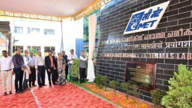
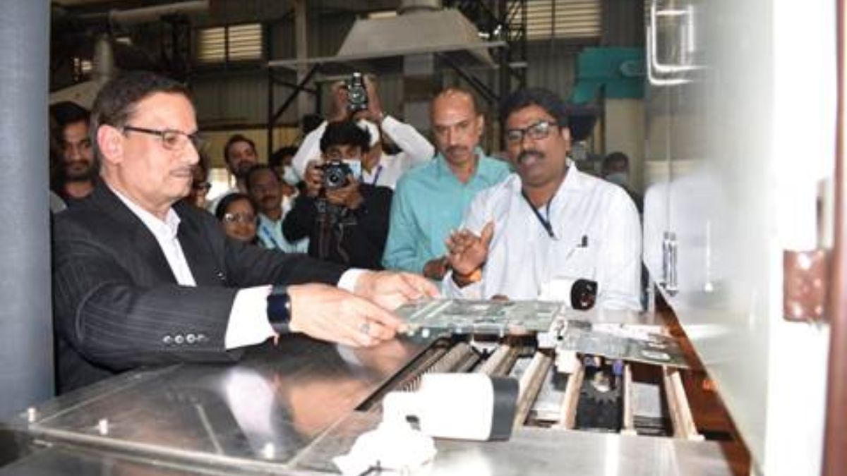
Shri Alkesh Kumar Sharma inaugurates PCB Recycling facility at C-MET, Hyderabad
Indigenously developed e-waste recycling technology gives a fillip to India’s Mission to Atmanirbharata and circular economy – Shri Alkesh Kumar Sharma
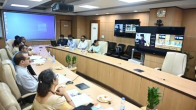
The Secretary, Ministry of Electronics and Information Technology (MeitY), Shri Alkesh Kumar Sharma inaugurated 1Ton/day PCB Recycling facility at the Centre for Materials for Electronics Technology (C-MET), in Hyderabad Yesterday.
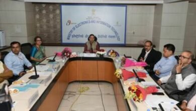
Talking on the occasion, Shri Alkesh Kumar Sharma mentioned that a circular economy approach towards e-waste management will play an important role in resource efficiency, reduction in pollution, recovery of precious materials and minimization of health hazards. He said that Ministry has introduced the SPECS scheme for helping e-waste recycling industries to set up their plant in India instead of sending the e-waste materials outside for recycling. He also said that the indigenously developed e-waste recycling technologies will give a fillip to India’s Mission to Atmanirbharata and circular economy.
Centre for Materials for Electronics Technology (C-MET) is an autonomous scientific society under the Ministry of Electronics and Information Technology, Government of India. It is having three R&D laboratories located at Hyderabad, Pune & Thrissur focusing on different thrust areas on critical electronic materials. C-MET, Hyderabad lab is focused on the development of high-purity, semiconductors and strategic materials including metals and alloys.
One of the major thrust areas of C-MET, Hyderabad is to develop environmentally benign e-waste recycling technologies to promote resource efficiency and a circular economy in the country. India generates around 3.2 million Tons per year of electronic waste which contains many precious materials like Gold, Palladium, Silver etc. in addition to hazardous materials which can cause irreparable health hazards to human beings. In this context, the development of environmentally benign process to address those issues are of paramount importance.
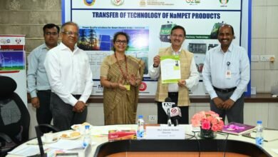
C-MET has established the Center of Excellence (CoE) on E-waste Management first of its kind in the country under the PPP model. CoE on E-waste management has developed all varieties of e-waste recycling technologies viz. spent PCB, Li-Ion Battery, Permanent magnet and Si-solar cells etc. The PCB recycling technology developed by CoE is at the Technology Readiness Level 6 stage and is now ready for commercialization. C-MET has not only developed recycling technologies but also designed and fabricated necessary processing equipment for the same.
Disclaimer: This is an official press release by PIB.