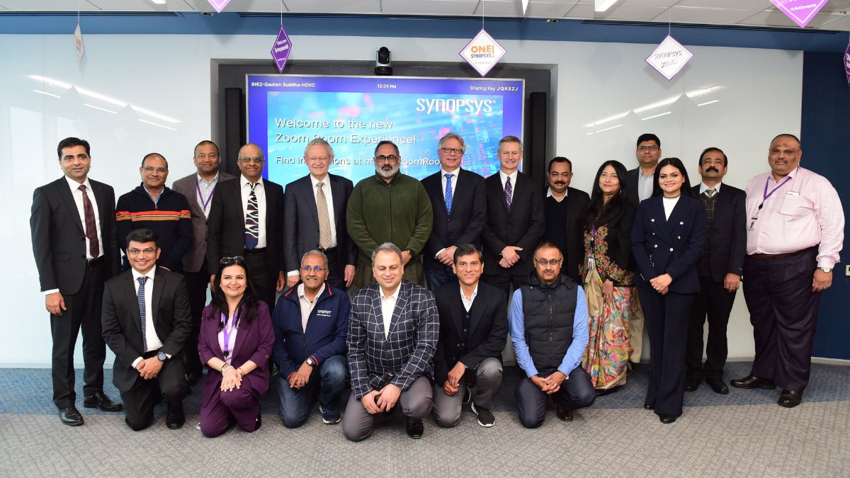
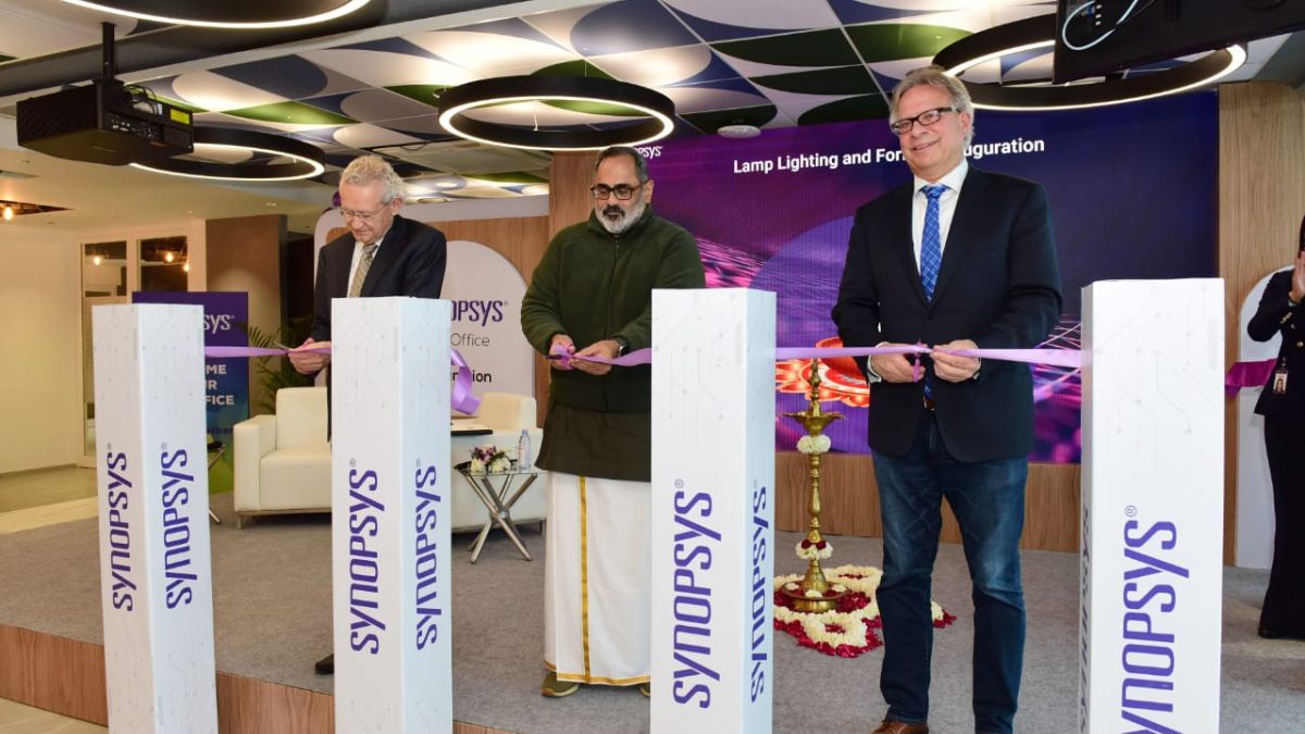
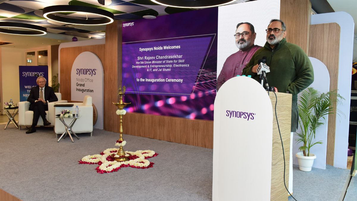
Yesterday, Shri Rajeev Chandrasekhar, Union Minister of State for Electronics and IT, Skill Development and Entrepreneurship, and Jal Shakti inaugurated Synopsys’ Chip Design Centre at DLF Tech Park in Noida. The event drew a distinguished audience, including senior leadership, employees, partners, and delegates from Synopsys.
During his address, the Minister said, “We are certainly living in the most exciting times yesterday. For somebody like me who has spent over 30-35 years in tech, I can say that it is absolutely thrilling to witness where India is heading in terms of the semiconductor space. The coming decade will see innovation-driven performances in our devices, products, and systems. There is significant headroom for innovation and growth yesterday, under the leadership of our Hon’ble Prime Minister Narendra Modi ji.
There is a lot of conventional wisdom about tech, its pace, and its dependence on more raw manufacturing processes. Both performance and manufacturing processes are being rewritten. It is as much about what the semiconductor ecosystem is going to be as it is about the innovation packaging, design, and the software that drives the innovation.”
The Minister further articulated that forging partnerships with global leaders such as Synopsys aligns seamlessly with India’s aspirations and future trajectory.
“The coming techade is going to be driven more by innovation in performance, systems, devices, and products. I come from an era where we used to perform logic synthesis manually. The rapid pace and velocity of innovation facilitated by companies like Synopsys are, in many ways, propelling the overall innovation of our tech and digital ecosystem. Therefore, I firmly believe that companies like Synopsys will become a significant player in shaping the future of technology,” the Minister added.

During his interaction with Dr Aart de Geus, founder of Synopsys, the Minister shared the Government of India’s approach to the semiconductor industry, emphasizing a dual focus on manufacturing and innovation. Expressing confidence in India’s natural aptitude for electronics and semiconductors, he affirmed the Govt’s commitment to building capabilities, aiming to lead in chips, devices, and product architecture.
He said, “We are looking at both the manufacturing and innovation sides of the industry. As we move into the future, I believe electronics and semiconductors come naturally to us, and that should be our focus. That is architectured and designed. This is our ambition, similar to many endeavours post-2014, we are indeed catching up on lost time. In semiconductor manufacturing, we are making significant progress. On the design and startup ecosystem fronts, we have made a lot of progress.
Having spent some time in the semiconductor ecosystem myself, what I have witnessed in the last 10 years is very different from before, and it is truly inspiring. From a government perspective, we believe we have a promising runway for growth in terms of talent, investment, and capabilities. Therefore, we view such partnerships as the glue and building blocks of our ambitions.”
Dr Aart de Geus acknowledged the parallel growth of Synopsys and India, expressing excitement about the future of the partnership. He highlighted the substantial investment and acquisition of startups that culminated in the establishment of the Noida center which will act as a hub for innovation.

“In the remarkable journey of India’s technological advancement, Synopsys has played a significant role, aligning seamlessly with the nation’s ambitions. In many ways, our growth has run parallel with India’s progress. With a third of our workforce based in India, we have invested significantly, exemplified by the Noida centre—a beacon of excellence that required substantial investments and the acquisition of eight startups.
This facility, a true Center of Excellence, serves as a cohesive hub. As we reflect on this partnership, it’s not merely a collaboration; it’s a shared home where ambitions and innovations thrive. India, now in its exciting phase of semiconductors and electronics, finds a perfect ally in Synopsys, marking the beginning of an even more promising chapter in technology and growth,” Dr Aart de Geus added.
Synopsys offers a diverse design portfolio, including silicon to software, which has played a pivotal role in generating $5.9 billion in revenue. As a dominant force in EDA tools and Interface, Foundation, & Physical IPs, Synopsys has secured a prominent position within the industry. Demonstrating confidence in Indian design talent, Synopsys has established the second-largest design centre in India, extending beyond its headquarters. This centre is now the workplace for around 6,000 engineers from India, constituting 27% of their global design workforce.
While it’s a well-established fact that 20% of global VLSI/Chip designers originate from India, the expanding presence of Synopsys in Noida, initially hosting 1650 engineers, underscores the growing ecosystem of fabless chip design and innovation in India. Synopsys’ Indian engineers play a pivotal role not only in every aspect of the semiconductor chip/IP Cores design cycle but also contribute significantly to the success stories of leading semiconductor companies. Virtually all chips designed by any company incorporate EDA/IP solutions in some capacity.
Disclaimer:This is an official press release by Pib.


